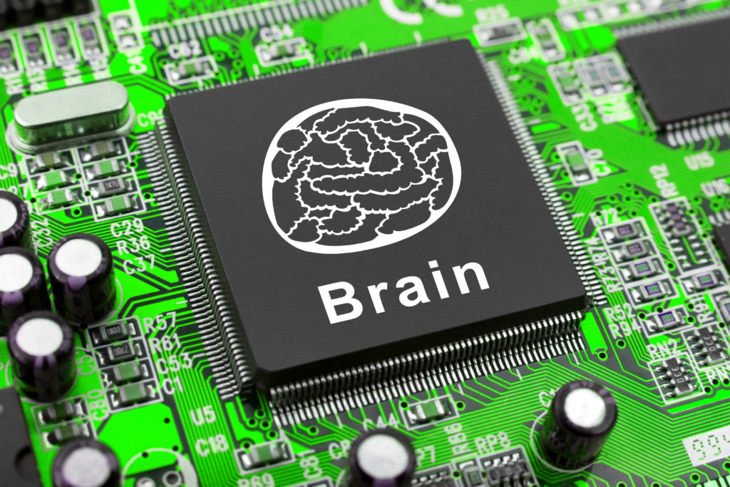
We often think of analytics on large scales, particularly in the context of large data sets (“Big Data”). However, there is a growing analytics sector that is focused on the smallest scale. That is the scale of digital sensors — driving us into the new era of sensor analytics.
Small scale (i.e., micro scale) is nothing new in the digital realm. After all, the digital world came into existence as a direct consequence of microelectronics and microcircuits. We used to say in the early years of astronomy big data (which is my background) that the same transistor-based logic microcircuitry that comprises our data storage devices (which are storing massive streams of data) is essentially the same transistor-based logic microcircuitry inside our sensors (which are collecting that data). The latter includes, particularly, the sensors inside digital cameras, consisting of megapixels and even gigapixels. Consequently, there should be no surprise that the two digital data functions (sensing and storing) are intimately connected and that we are therefore drowning in oceans of data.
But, in our rush to crown data “big”, we sometimes may have forgotten that micro-scale component to the story. But not any longer. There is growing movement in the microchip world in new and interesting directions.
I am not only talking about evolutions of the CPU (central processing unit) that we have seen for years: the GPU (graphics processing unit) and the FPGA (field programmable gate array). We are now witnessing the design, development, and deployment of more interesting application-specific integrated circuits (ASICs), one of which is the TPU (tensor processing unit) which is specifically designed for AI (artificial intelligence) applications. The TPU (as its name suggests) can perform tensor calculations on the chip, in the same way that earlier generation integrated circuits were designed to perform scalar operations (in the CPU) and to perform vector and/or parallel streaming operations (in the GPU).
Speeding the calculations is precisely the goal of these new chips. One that I heard discussed in the context of cybersecurity applications is the BPU (Behavior Processing Unit), designed to detect BOI (behaviors of interest). Whereas the TPU might be detecting persons of interest (POI) or objects of interest in an image, the BOI is looking at patterns in the time series (sequence data) that are indicative of interesting (and/or anomalous) behavioral patterns.
The BOI detector (the BPU) would definitely represent an amplifier to cybersecurity operations, in which the massive volumes of data streaming through our networks and routers are so huge that we never actually capture (and store) all of that data. So we need to detect the anomalous pattern in real-time before a damaging cyber incident occurs!

You can continue reading the long version of this article and learn more about the growing class of new analytics ASIC processors in my article “Sensor Analytics at Micro Scale on the xPU” at the Western Digital DataMakesPossible.com blog site.
Learn more about Machine Learning for Edge Devices at Western Digital here: https://blog.westerndigital.com/machine-learning-edge-devices/
Finally, see what’s cooking in Western Digital’s new Machine Learning Accelerator here: https://blog.westerndigital.com/machine-learning-accelerator-embedded-world-2019/
Source for graphic: https://www.sigarch.org/a-brief-guide-of-xpu-for-ai-accelerators/


